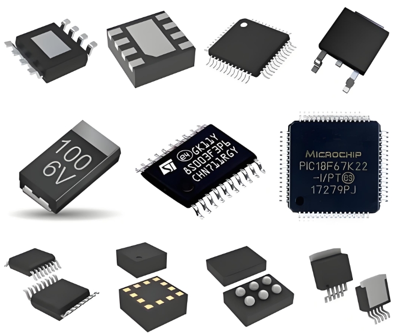
**Unveiling the AD7541AKNZ: A Comprehensive Technical Overview of the Precision 12-Bit Multiplying DAC**
In the realm of high-precision digital-to-analog conversion, the **AD7541AKNZ** stands as a seminal and enduring component. This 12-bit multiplying digital-to-analog converter (DAC), originally introduced by Analog Devices, has established a reputation for reliability and performance in a wide array of critical applications. This article provides a detailed technical exploration of its architecture, key features, and operational principles.
At its core, the AD7541AKNZ is a **monolithic CMOS multiplying DAC**. Unlike conventional voltage-output DACs, a multiplying DAC's reference input is an analog variable, allowing the device to function not only as a precision DAC but also as a digitally controlled attenuator or a four-quadrant multiplier. The AD7541AKNZ is designed with a precision laser-trimmed thin-film R-2R ladder network, which is the source of its **exceptional linearity and accuracy**. This architecture ensures minimal non-linearity error, a critical parameter for maintaining signal integrity across the entire digital code range.
The device operates on a simple yet effective current-switching principle. The 12-bit digital word, applied to its inputs, controls an array of CMOS current switches. These switches steer current either to the output node (I_OUT1) or away from it (I_OUT2). The output is thus a precise current proportional to the product of the digital code and the analog reference voltage applied to the V_REF pin. This **current-output format** provides significant design flexibility; by using an external operational amplifier, the designer can easily configure the output for unipolar or bipolar voltage ranges, as well as for various scaling factors.

A defining characteristic of the AD7541AKNZ is its **four-quadrant multiplication capability**. Since both the digital input and the analog reference can be bipolar signals, the output can represent the product of these inputs in all four quadrants of the operational plane. This makes it indispensable in complex modulation schemes, waveform generation, and automatic gain control circuits. Furthermore, its CMOS construction grants it **low power consumption**, typically drawing less than 2mW from a single +15V supply, making it suitable for portable and power-sensitive equipment.
Other notable specifications include a fast settling time to within ±1/2 LSB and high compliance output voltage range. While it requires external precision components—namely a reference voltage source and an output op-amp—to form a complete voltage-output DAC, this very requirement allows engineers to tailor the circuit's speed, accuracy, and output range to the specific needs of the application.
The AD7541AKNZ has found its place in numerous demanding fields, including **professional audio equipment** for digital volume control, **precision instrumentation** for calibration and programmability, and **industrial process control systems** where accurate analog command signals are paramount. Its robustness and performance have ensured its longevity in the electronics component landscape.
**ICGOODFIND:** The AD7541AKNZ remains a benchmark for precision 12-bit multiplying DACs, offering designers a unique combination of **flexibility, accuracy, and proven reliability** for complex analog computation and signal conditioning tasks.
**Keywords:** Multiplying DAC, 12-Bit Resolution, Four-Quadrant Multiplication, R-2R Ladder, Current Output.
